20+ fir filter block diagram
Finite Impulse Response. Of the above FIR filter is.
What Is Fir Filter Fir Filters For Digital Signal Processing
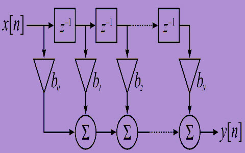
Block Diagram Representation Input-output relation of an LTI system can be realized using different computational algorithms.

. In the digital signal processing system the use of FIR short form is one type of filter whose impulse response is of finite duration the reason of it settles zero in finite. 5120 Draw the block diagram in the direct form for the FIR. To implement the filter.
FIR filter block diagram. A sample delay line and a set of coefficients. Usually these filters are designed with a multiplier adders and a series of.
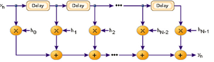
Of memory blocks required in the filter implementation Filter Length L M1. The terms represent unit delays. Computer Science questions and answers.
There are several different realization block diagram of FIR system. Filter Order M. Draw the block diagram of 3rd order FIR filter.
Structurally FIR filters consist of just two things. The shaping filter is based on a direct FIR but what makes it different is the delay line instead of having one delay. Of samples required in calculating the output M from memory past and one.
DIRECT FORM The difference equation of Direct Form structure can be described as below. Put the input sample into the delay line. Discover by subject area.
Logical Structure of FIR Filter. A FIR filter is used to implement almost any type of digital frequency response. Multiply each sample in the delay.
FIR filter block diagram. Block diagram of an Interpolated FIR filter. Note that while this representation for a delay element is common and widely accepted in the signal processing community the specification of delay in.
Write the difference equation for the filter and find out the. A finite impulse response FIR filter is a filter structure that can be used to implement almost any sort of frequency response digitally. Basic IIR Digital Filter Structures 1.
An FIR filter is. 5120 Draw the block diagram in the direct form for the FIR filter when the frequency response is given by.

Fir Filter Block Diagram Download Scientific Diagram

4 Block Diagram Of A Iir Filter Download Scientific Diagram

Block Diagram Of The Fpga Based Fir Filter Download Scientific Diagram

The Proposed Structure Of The Da Based Fir Filter For Fpga Download Scientific Diagram
Block Diagram Of The Fir Filter With Sdm Modulated Input Signal Download Scientific Diagram

7 Block Diagram Of A 4 Tap Fir Filter Download Scientific Diagram
What Is Fir Filter Fir Filters For Digital Signal Processing

Block Diagram Of Digital Fir Filter 22 Download High Quality Scientific Diagram
Block Diagram Of Fir Filter Coefficient Calculation Algorithm Download Scientific Diagram

Block Diagram Of Fir Filter Structures A Tapped Delay Lines And B Download Scientific Diagram

3 Block Diagram Of A Fir Filter Download Scientific Diagram

Basic Block Diagram Of Fir Filter Download Scientific Diagram

9 Fir Filter Block Diagram Download Scientific Diagram
![]()
Structure Of Fir Filter A Transposed Form B Fir Filter Using A Download Scientific Diagram

Block Diagram Of The Fpga Based Fir Filter Download Scientific Diagram

Rf Canceller Analog Fir Filter Block Diagram Download Scientific Diagram

Schematic Diagram Of The Fir Filter Download Scientific Diagram